Posted on

Cadence Achieves TÜV SÜD’s First Comprehensive “Fit for Purpose – TCL1” Certification in Support of Automotive ISO 26262 Standard

SAN JOSE, Calif., October 11, 2017—Cadence Design Systems, Inc. (NASDAQ: CDNS) today announced that it has achieved the industry’s first comprehensive “Fit for Purpose – Tool Confidence Level 1 (TCL1)” certification from TÜV SÜD, enabling automotive semiconductor manufacturers, OEMs and component suppliers to meet stringent ISO 26262 automotive safety requirements. To achieve certification, Cadence provided its tool and flow documentation to TÜV SÜD for evaluation, and TÜV SÜD confirmed the Cadence® flows are fit for use with ASIL A through ASIL D automotive design projects. The functional safety documentation kits cover analog and mixed-signal, digital front-end and verification, digital implementation and signoff, and PCB flows comprised of nearly 40 tools, offering the broadest EDA-certified tool and flow documentation to support the automotive industry.

Cadence customers can easily access the tool and flow documentation and TÜV SÜD technical reports via the Cadence Automotive Functional Safety Kits at www.cadence.com/go/iso26262cert.

Based on the growing importance of EDA solutions for the automotive safety market, both TÜV SÜD and Cadence determined that it was necessary to add a new certification level to further ease the automotive chip designer’s process for achieving ISO 26262 compliance. The Cadence flow-level certification is verifiable via the TÜV SÜD certification database.

Under this new certification model, certificates have been issued for each tool flow documentation kit and have a five-year validity. TÜV SÜD plans to review updates to the tool flows and their impact on ISO 26262 compliance at least once a year.  

 “We collaborated with Cadence and determined that establishing a documentation certification program could benefit customers applying the Cadence tool chains in ASIL A through ASIL D projects,” said Günter Greil, head of the generic functional safety components department at TÜV SÜD. “Automotive semiconductor manufacturers, OEMs and component suppliers are under pressure to meet aggressive delivery deadlines, while also achieving compliance with the ISO 26262 standard. The new documentation program allows customers to reduce the time spent on tool qualification so they can keep their focus on product innovation.”

The tool flow documentation that achieved the TÜV SÜD “Fit for Purpose – TCL1” certification and is included with Cadence Automotive Functional Safety Kits is as follows:

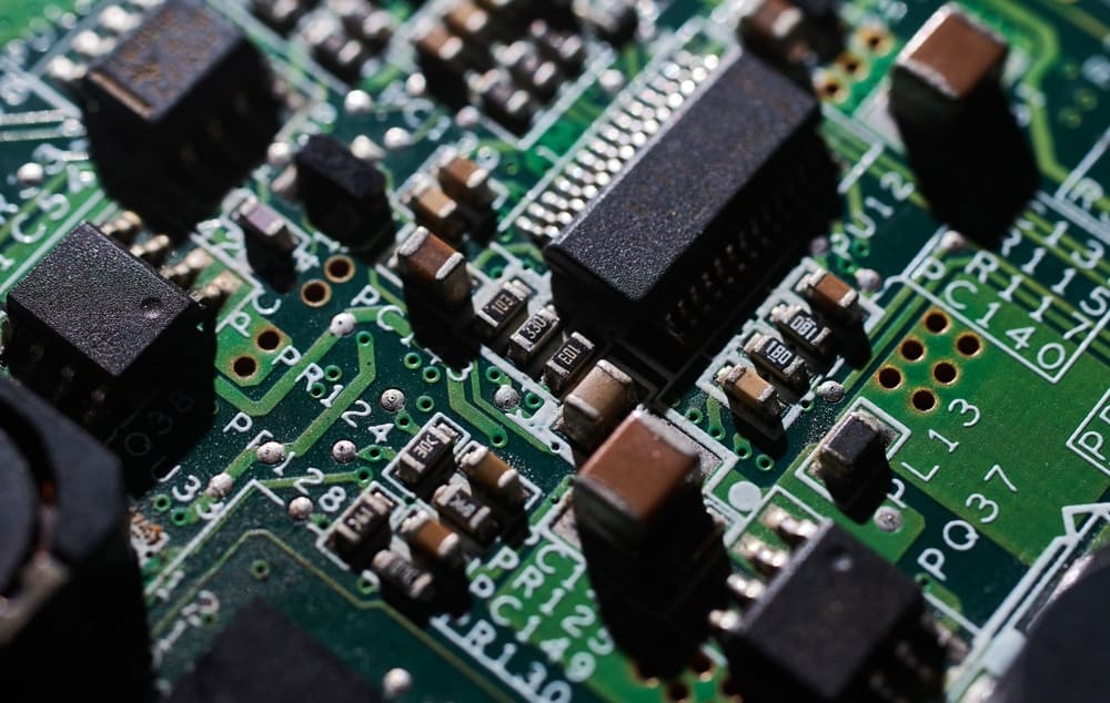
PCB design and verification flow: This new certification for PCB design includes everything from design authoring to simulation to physical realization and verification using the Cadence OrCADÒ, PSpiceÒ and AllegroÒ product suites. The high-performance design entry, simulation and layout editing tools included with these suites provide an integrated environment for design engineers to validate the safety specifications against individual circuit specifications for design confidence.

Analog/mixed-signal design, implementation and verification flow: This flow brings transistor-level designs from creation and simulation through physical implementation and verification using the Cadence VirtuosoÒ ADE Product Suite and the SpectreÒ Circuit Simulation Platform. The Cadence Virtuoso ADE Verifier provides design engineers with an integrated means to validate the safety specifications against individual circuit specifications for design confidence.

Digital implementation and signoff flow: This flow covers RTL-to-GDSII implementation and signoff. The Cadence Virtuoso LiberateÔ Characterization Solution is new to this flow and is incorporated with the 13 other pre-existing tools including the Cadence InnovusÔ Implementation System, GenusÔ Synthesis Solution, ModusÔ Test Solution, TempusÔ Timing Signoff Solution, QuantusÔ QRC Extraction Solution and VoltusÔ IC Power Integrity Solution for the implementation and signoff of automotive designs.

The digital front-end design and verification flow’s documentation kit has been evaluated and confirmed to be compliant with ISO 26262, and is expected to achieve certification during Q4 2017. The flow documentation kit covers specification to RTL design to verification. The front-end digital tools include the Cadence GenusÔ Synthesis Solution and ConformalÒ Equivalence Checker. Functional and safety verification capabilities are provided by the Cadence Verification Suite, which includes the Cadence JasperGoldÒ Formal Verification Platform, XceliumÔ Parallel Logic Simulator (to be added to the flow documentation in Q4 2017), PalladiumÒ Z1 Enterprise Emulation Platform, ProtiumÔ FPGA-Based Prototyping Platform, vManagerÔ Metric-Driven Signoff Platform and the IndagoÔ Debug Platform (to be added to the flow documentation in Q4 2017). 

“Cadence’s flow-level approach to documentation aims to make it much simpler for automotive component suppliers to achieve compliance with the ISO 26262 standard,” said Raja Tabet, corporate vice president, Emerging Technologies at Cadence. “By providing pre-certified documentation, Cadence is greatly reducing the effort needed for customers to achieve their certification goals. Customers appreciate the flexibility and expediency that this approach allows. Partnering with TÜV SÜD on the flow-level certification of our documentation and the creation of the new ‘Fit for Purpose – TCL1’ certification mark demonstrates our commitment to the automotive market and support for semiconductor manufacturers, OEMs and component suppliers that are working to gain an edge with their respective solutions.”

About Cadence

Cadence enables electronic systems and semiconductor companies to create the innovative end products that are transforming the way people live, work and play. Cadence software, hardware and semiconductor IP are used by customers to deliver products to market faster. The company’s System Design Enablement strategy helps customers develop differentiated products—from chips to boards to systems—in mobile, consumer, cloud datacenter, automotive, aerospace, IoT, industrial and other market segments. Cadence is listed as one of Fortune Magazine’s 100 Best Companies to Work For. Learn more at cadence.com.

Posted on

EMA Introduces E-Learning and OrCAD Certification To Improve and Validate OrCAD User Proficiency

Rochester, NY (April 25, 2017) – EMA Design Automation®, a full-service provider and innovator of Electronic Design Automation (EDA) solutions, has just released a new E-Learning training platform and an OrCAD certification program to help OrCAD users improve their proficiency with the toolset and earn a certification to demonstrate their level of knowledge.  “Quite often, customers will ask me if I know of any qualified engineers that they could hire and put to work immediately,” said Manny Marcano, president and CEO of EMA.  “Because of this certification program, with a simple web search and a review of LinkedIn certification credentials, hiring managers can easily find qualified OrCAD engineering candidates.”

The new E-Learning platform allows students to learn at their own pace.  The E-Learning modules cover the same material as their classroom counterparts, providing comprehensive training resources which include both videos and labs.  Students use their own computers and access the guided training via the internet. 

All EMA training includes the opportunity to take the OrCAD certified exam for the tool covered in the course.  However, taking the course isn’t required to take the exam.  Experienced OrCAD users can purchase an exam for a small fee if they believe they already possess the knowledge required for the particular subject.  Anyone who does not pass an exam can continue studying and retake the exam when they feel they are ready.  They can also apply the cost of the exam to an EMA training course.  Students who pass the exam will receive an OrCAD Certified™ certificate for the tool they have mastered, as well as being able to list the certification on their LinkedIn page, business cards, resumes, and biographies.  The certificate will also include the software version of the tool that was passed to help identify those with the latest expertise.

“Our existing courseware has been tremendously successful,” added Marcano.  “In fact, 98% of the students agreed that the EMA training they received would greatly improve their work performance, and 9 out of 10 students confirmed the class they attended exceeded their expectations.  With the addition of the OrCAD certification exams, OrCAD aficionados can proclaim their proficiency, and hiring managers have an added tool to ensure that they get the best candidates available.”

For more information about the EMA E-Learning and OrCAD Certification, visit go.ema-eda.com/orcad-certified.

OrCAD Certification

OrCAD Certified

Become OrCAD certified and promote your expertise.

Accelerate Success and Proclaim Your OrCAD Proficiency

Our OrCAD® certification program is included in the price of your Capture, PSpice, or PCB Editor class and is designed to help you demonstrate proficiency in OrCAD tools. Become OrCAD certified and validate your skills, stand apart from your peers, and expand career opportunities.

Benefits of Certification

  • Gain Professional Credibility
  • Ensure a Solid Foundation in OrCAD Product Knowledge
  • Improve Productivity
  • Validate Expertise

Display Your Certification Where it Matters

Users who pass certification training will receive an official certificate and OrCAD certification badge image they can display on company websites, social media accounts, etc.—validating their ability to plan, design, and implement our software. Show your customers, peers, and employers you have the knowledge to successfully utilize OrCAD products.

Currently Available for the Following Classes

Ready to Sign Up For A Class?

Visit our classes page to learn more about how you can maximize the return on your OrCAD purchase through training.


View Class Schedule

Need more info?

The EMA Team will be happy to assist you.

Contact Us

Posted on

Plugfest 2024: Event Guide

Plugfest 2024, checking your USB device compliance

At Plugfest 2024, you can verify your USB device compliance

The global electronics market exceeds a trillion dollars, and is projected to continue to grow by nearly 3% annually for the foreseeable future. And, there is tremendous competition for market share among OEMs, ODMs, and others that design and develop circuit boards. However, the requirement of interconnectivity between components and devices from various manufacturers to ensure reliable operation and quality performance creates a sense of camaraderie at events such as plugfests.

Plugfests, as the name implies, are opportunities for designers, developers, manufacturers, and others to plug their product into a device or product from another company and put it to the test. The primary objective of these industry gatherings is typically to validate a product’s compliance with a particular standard(s). For USB boards and devices that require USB compliance testing, Plugfest 2024 events that are sponsored or sanctioned by the USB-IF provide opportunities to verify that your product meets USB compliance standards. Capitalizing on these industry plugfests; however, requires preparation.

USB Plugfest 2024 Events

Below is a list of scheduled plugfests for 2024.

PLUGFEST 2024 EVENTS

Plugfest Event

Dates and Location

USB Compliance Testing

USB-IF Compliance Workshop #133

January 29 – February 2, 2024

Burlingame, CA

PD 3.1 E-Markers, Silicone and Power Bricks, Shared Capacity Chargers, Power Banks and Power Sinking Devices

International Plugfest 2024

26 February – 01 March, 2024

London, UK

Includes compliance testing for USB, MIPI, HDMI and other protocols for A/V applications.

NOTE: Plugfest events may be scheduled at any time throughout the year.

Why Attend a USB Plugfest in 2024?

Many organizations sponsor plugfests or compliance testing events throughout the year. And there are benefits to attending a USB plugfest regardless of where you are in PCBA development.

REASONS TO ATTEND PLUGFEST 2024

Benefits

PCB Development Stage

  1. Test your product’s
    functionality/compatibility
    with other USB devices.

Design, Manufacturing, Testing

  1. Verify your product’s compliance
    with a particular USB standard.

Design, Manufacturing, Testing

  1. Select components and devices
    for use with your USB product.

Design

  1. Learn current USB standards
    and technology innovations.

Design

  1. Help with the development of
    USB standards.

Design

As the list above illustrates, testing and verifying your product is the main reason for attending a plugfest. However, several benefits can be advantageous to your PCBA design process. Note that testing and compliance verification can be done at any plugfest. However, testing for certification can only be done at a USB-IF authorized independent testing laboratory (ITL), Platform Interoperability Lab (PIL), or plugfest like Compliance Workshop #133.

The organization’s Plugfest 2024 focuses on USB 3.1 power delivery (PD 3.1), including the following:

USB-IF Plugfest 2024 Compliance Testing Categories

  • USB PD 3.1 
    • Power bricks
    • Only silicon
    • E-markers
  • USB 4 E-markers
  • Shared capacity chargers
  • Sinking devices (single and multi-port)
  • Power banks (including DRP)

As the above categories exhibit, plugfests are specific standard events. Therefore, it is crucial to adequately prepare to take advantage of the benefits these events offer.

Optimizing a USB Plugfest for Your PCBA Development

Plugfests are organized to use compliance testing to ensure interconnected USB products operate smoothly and perform reliability irrespective of the manufacturer/distributor. Maximally leveraging these events, which is best achieved by following the guidelines listed below, can also be a significant asset for optimizing your development process.

Preparation Guidelines for a USB Plugfest 2024

  •  Know the specific standard focus, including sub-categories 
    As is the case for the USB-IF Plugfest 2024, these events typically have a constrained focus. For example, USB 3.1 Gen 1 hubs, hosts, and compound parts are not eligible for testing, while USB 3.1 PD products are.

  •  Know the explicit certification requirements for your product
    Different product types have different test regimens and metrics that are evaluated. Therefore, it is essential to know what these are to prepare for the tests.

  •  Use software tools to pretest your design for compliance
    The best way to prepare for success at a plugfest is to pretest. Care must be exercised here to ensure that your choice of product development software can emulate the test regimens used to test/verify the compliance of your product.

    To learn how to verify USB compliance during design and avoid wasteful manufacturing costs and time consuming redesigns, see this eBook.

Market competitiveness, tight development schedules, and other profitability issues are major concerns for new product introductions (NPI). For USB products, testing and verifying compliance can significantly impact design and development costs. One way to minimize these and help optimize ROI is to take advantage of events like Plugfest 2024.

EMA Design Automation is a leading provider of the resources that engineers rely on to accelerate innovation. We provide solutions that include PCB design and analysis packages, custom integration software, engineering expertise, and a comprehensive academy of learning and training materials, which enable you to create more efficiently. For more information on Plugfest 2024 and how we can help you or your team innovate faster, contact us.

Posted on

Optimizing the Electronic New Part Introduction (NPI) Process

CIP Flow Diagram
CIP Flow Diagram
Electronic New Part Introduction Process (NPI) in CIP

During the PCB design process, it’s highly improbable that all the parts required for the design are already found in your company’s part database due to the constant innovation of electronic components. For PCB components to keep up with industry and design standards, continuous improvement to be faster, smaller, and operate at lower power is required. This results in a consistent flow of new components to the market and your designs. Incorporating new components into a design or system is referred to as the electronic New Part Introduction (NPI) process. Throughout this process, many steps need to occur to ensure successful integration of new electronic components into a design:

NPI StepDescriptionResponsible Party*
Define Component RequirementsDefine the requirements of the new part including functionality, performance specifications, and specific features.Designer
Market ResearchIdentify suitable components that meet the defined requirements. Consider cost, availability, and compatibility with existing components.Component Engineer or Designer
Vendor SelectionSelect reputable and reliable vendors to source components. Consider quality and lead times.Component Engineer, Designer, or Purchasing
Component EvaluationEvaluate the selected components to ensure they meet the required specifications. May involve testing samples, reviewing datasheets, conducting simulations.Designer
Model Creation and ValidationCreate schematic symbols and PCB footprints. Verify accuracy and integration between both.Component Engineer or Designer
Ensure Regulatory ComplianceEnsure components will comply with regulatory standards and certifications.Component Engineer, Project Manager, or Librarian
Add Component to DatabaseEnter all parametric information, models, supply chain data, and vendor information into the component database.Component Engineer, Project Manager, or Librarian
Release the ComponentVerify all component information including parametrics, models, datasheets, vendors, and supply chain information then release the component for use in designs.Project Manager or Librarian
Design IntegrationIntegrate new components into the design. Update the schematic, layout, and documentation.Designer
Update Supply Chain InformationUpdate vendor information, lifecycle, and supply chain data to guarantee parts used in designs are available. This is an on-going task.Component Engineer, Project Manager, or Librarian

*Roles responsible for steps in the Electronic New Part Introduction (NPI) process may vary based on company standards and practices.

While the electronic NPI process is critical to design success, if performed inefficiently it often results in delays to the design process. After the designer requests a new part, the time it takes to create the associated models, perform part research, add the component to the company database, and verify the accuracy of component data can have a detrimental impact on time-to-market and project deadlines.

Electronic New Part Introduction (NPI) Process with OrCAD CIP

Electronic New Part Introduction (NPI) Process with OrCAD CIP

OrCAD Component Information Portal (CIP) streamlines the NPI process while creating a centralized library for part selection and management. OrCAD CIP provides direct integration to distributors and trusted data partners, allowing designers to research and select parts without leaving their CAD tool. When requesting a new part, parametric and supply chain information is pulled directly from distributors, saving time by eliminating manual entry and minimizing human-errors. A temporary part is generated while the part is reviewed and CAD models are created, allowing the designer to continue with the schematic. Customizable user roles and permissions coupled with automated alerts ensures the correct team members are editing and approving components while keeping the NPI process on track.  With seamless integration between the project and the component database, designers are automatically notified of component changes or approvals and updates are applied as needed. While the electronic NPI process in OrCAD CIP greatly improves efficiency, there is still one hold-up – CAD model creation and verification.

Solving the CAD Model “Problem”

The complexity of today’s electronic components is necessary to meet the technological demands of cutting-edge products; however, this also increases the complexity of CAD model creation. With hundreds of pins and intricate device packaging, schematic symbols and PCB footprints can take hours if not days to complete. These models then need to be verified for accuracy and compliance to either company or industry (ANSI and IPC) model standards. In many product designs, 3D models and simulation models must also be created or sourced to achieve full system verification. To decrease the model creation and validation demands, component models can be sourced from reliable, CAD libraries such as Ultra Librarian. Typically, this involves searching the component model database, downloading the required models, and manually sharing the models with the CAD librarian or project manager; however, new integrated access to Ultra Librarian within OrCAD CIP automates this process.

Fully Automated Electronic NPI with OrCAD CIP and Ultra Librarian

Verified Ultra Librarian Symbols and Footprints to accelerate the electronic new part introduction (NPI) process
Incorporating Pre-Built CAD Models into the NPI Process with CIP

OrCAD CIP has now incorporated direct integration to Ultra Librarian within the electronic NPI process. During new electronic part requests, designers can now access, review, and associate fully validated component models. This allows design teams to achieve a fully automated and efficient NPI process with OrCAD CIP and Ultra Librarian by:

  • Achieving an automated process to manage NPI from start to finish
  • Performing part resource, selection, and addition directly inside your CAD system for ultimate productivity
  • Accessing live distributor and supply chain data without leaving your design environment
  • Continuing the design process while the new part is reviewed and approved with temporary parts
  • Accessing pre-built, verified CAD Models through Ultra Librarian
  • Easily associating CAD models to new parts
  • Adding parts through a managed configurable process
  • Eliminating error-prone manual entry of component parametrics
  • Tracking new parts added with a detailed history
  • Integrating with a PLM or other downstream systems
  • Configuring user permissions, roles, and alerts to keep the NPI process on-track and ensure all stakeholders are informed

Learn more about the benefits of implementing a centralized part selection and management system with OrCAD CIP.

Posted on

Creepage and Clearance Standards

Creepage and clearance standards are required to address the component density common on today’s PCBAs

As circuit board size decreases and functionality and capability demands increase, circuit board real estate becomes extremely valuable. Footprint pads, part pins, traces, vias, and other circuit board elements all need adequate space. Not to mention, circuit board fabrication and PCB assembly processes that require spacing for solder masking, solder flow, depanelization, etc. For high-voltage circuit boards, adequately addressing spacing is even more critical due to the significant damage that large voltages, currents and powers can create.

Consequently, there are regulations and guidance that emphasize the need for adequate spacing between conductive elements is in place. This is especially true for multilayer PCB designs, where increased layers are used to support smaller board area sizes. Fortunately, there are industry organizations that regularly publish rules and guidelines to address spacing on PCBAs, including creepage and clearance standards that are focused on trace routes. Knowing and following these standards is a key to designing safe boards that satisfy your performance objectives and will reliably perform over their lifecycle. 

The Creepage and Clearance Standards to Know

The most common considerations with any board design for engineers throughout the PCBA design process are how to minimize electromagnetic interference (EMI) and maximize electromagnetic compatibility (EMC). For high-voltage applications, EMI or unwanted noise and excessive emissions–a major EMC issue–are also important. However, at elevated voltage/current/power levels, safety is the greatest concern.

High voltages can be the catalyst for damaging surface tracking, where an alternate current path between conductors is created through the board’s insulation. These “effective short circuits” can damage components, the PCB and lead to fires that threaten other boards, systems and even nearby users. 

The most effective means of mitigating these contingencies is to have sufficient distance between sources and potential areas that can be affected. Consequently, there are several industry publications that include recommendations, guidelines, and/or requirements for PCB creepage and clearance distances. The most important of these are listed below.

IMPORTANT PCB CREEPAGE AND CLEARANCE STANDARDS

Standard

Description | Importance

IPC-2221A

Generic Standard on Printed Board Design

Includes specifications for spacing between surface conductors; space requirements for PCB stackup dielectrics and conductors; and clearances for components, edge connectors, and board extraction.

IPC-9592B

Requirements for Power Conversion Devices for the Computer and Telecommunications Industries 

Includes spacing requirements applicable to circuit boards that include DC-DC, DC-AC, power supplies, and other conversion devices used in the computer and telecommunications industries. 

IEC 62368-1

Testing and Certification

Includes creepage and clearance distance requirements for boards used in information technology systems, and information for testing and certifying your design.

*Replaces the well-known IEC-60950-1 Information Technology Equipment standard.

The publications listed above are not exhaustive creepage and clearance standards for all circuit board designs. However, they do contain industry requirements that are applicable to the most common PCBA design types, where EMI, EMC, and safety are primary considerations. In addition to knowing what creepage and clearance standards to use, it is also essential to understand the difference between creepage and clearance for circuit boards.

Creepage is the shortest distance between two adjacent conductors along the surface of the circuit board insulating material. 


Clearance is the shortest distance between two adjacent conductors through the air.

Above, creepage and clearance refer to the distance between any conductive board elements. For example, this includes trace to trace, conductor pad to trace, via annular ring to pad, etc. Often, the clearance distance is shorter than the creepage distance due to trace routing around board obstacles, such as components or drill holes. 

PCBA Creepage and Clearance Design Best Practices

Spacing requirements are an essential part of your CM’s DFMA rules and guidelines that should be integrated into the PCBA design process. Doing so is essential for the manufacturability of your board. These rules should include and/or be consistent with industry creepage and clearance standards, which can be ensured by following the best practices listed below.

Creepage and Clearance Design Guidelines

  •  Determine which creepage and clearance standards and distances apply to your board type
  •  Setup your PCB design software DRC creepage and clearance constraints according to the appropriate standard specification(s)
  •  Perform DRC checks often and correct any spacing violations identified during your PCB layout design process by
  •  Adding a slot between conductors to increase creepage distance without modifying the locations of any conductors
  •  Adding vertical insulation barrier between conductors to increase creepage distance
  •  Changing the orientation of a conductive element–this may require rerouting traces
  •  Replacing the conductor with an alternative part with similar performance criteria
  •  Use PCB simulation to check/verify that your creepage and clearance specifications meet industry safety standards for all voltage levels 

By following the guidelines above, including adhering to the distance constraints from the proper industry creepage and clearance standards, you can make sure your board is designed to maximize component, board and user safety, as well as minimize issues like EMI and meet your performance objectives. This is best accomplished by utilizing an advanced PCB design package or incorporating a product design software solution that includes dedicated functionalities–for example, creepage and clearance vision with color-coded overlays–to help you optimize your development process.

EMA Design Automation is a leading provider of the resources that engineers rely on to accelerate innovation. We provide solutions that include PCB design and analysis packages, custom integration software, and engineering expertise, which enable you to create more efficiently. For more information on how best to incorporate PCB creepage and clearance standards into your design process and how we can help you or your team innovate faster, contact us.

EMA Support Plus

EMA Support+

Support+

Get more value for your maintenance with exclusive benefits from the PCB Design experts at EMA

Get more value for your maintenance with exclusive benefits from the PCB Design experts at Parallel Systems and EMA

Get more value for your maintenance with exclusive benefits from the PCB Design experts at Sunstream and EMA

Get more value for your maintenance with exclusive benefits from the PCB Design experts at Anacom and EMA

The 5-Star EMA Support You Know and Depend On Plus More

Improve your productivity, solve problems faster and work more effectively with access to EMA experts, training, and technology to optimize your Cadence design experience. All available for FREE to active maintenance EMA customers.

Exclusive EMA Customer Advantages

With over 30 years of PCB Design and Cadence technology expertise the EMA team has put together the resources and tools you need to be successful. All included with your current maintenance at no extra cost.

1

EMA Toolkit

Improve your productivity, solve problems faster, and work more effectively with access to exclusive EMA technology to enhance your Cadence design experience.

CircuirFit-App-Icon.png

CircuitFit

Easily calculate the space on the board occupied by components and determine whether any larger components need be replaced during the schematic design with the CircuitFit app.

Highlight-by-Property-App-Icon.png

Highlight Part

Automatically color-code parts by a specific property (ex: lifecycle, availability, etc) on the schematic canvas to easily identify components with the Highlight Parts by Property app.

PCB-Clustering-App-Icon.png

PCB Clustering

Complete the PCB layout quickly and efficiently with automatic clustering and placement of components using the PCB Clustering App.

Find-In-Design-App-Icon.png

Find in Design

Easily find every design where specific components are used by searching the design repository and sub folders with the Find in Design App.

MicrosoftTeams-image-25.png

CIS BOM Template

Quickly create the desired Bill of Materials from Capture CIS using predefined Excel Templates and the CIS Template-Based BOM App.

testpoint-icon-border

Testpoint App

The Test Point Back Annotation App allows for automated addition of testpoints to nets in the schematic using a testprep file from PCB Editor.
multipin-connector_app

Multi-Board Connector App

Efficiently verify pin-outs between mating connectors from two different schematics to ensure accuracy and proper functionality of your PCB product with the Multi-Board Connector Pin Check App.

AND MORE COMING!

2

EMA eLearning

Make the most of your Cadence investment and stay up on the latest techniques with our extensive training library.

eLearning

Learn at your own pace with self-guided, online training classes complete with videos, labs, and comprehensive training materials.

Certification

Ensure a solid foundation of OrCAD knowledge, validate your expertise, and gain professional credibility with OrCAD Certifications.

Workshops

EMA’s workshops provide an in-depth training with interactive presentations, demonstration videos, and quizzes to elevate your knowledge and help you make the most out of your OrCAD software.

Tutorials

Quickly learn how to perform specific tasks throughout the design process with step-by-step instructions and demonstration videos for OrCAD features.

3

EMA Knowledgebase

Leverage our 30 years of supporting Cadence products with our comprehensive solution knowledgebase full of solutions, tips, and guides to help answer your questions fast and accurately.

Claim Your EMA Support+ Benefits

Frequently Asked Questions

Since our start EMA has built our business on being customer centric and ensuring we add value to help you be successful. As a result, we have been providing these kinds of value -add services to customers individually for years. The purpose of this program is to formalize these benefits and make sure they are available to all our users. We are really excited to share the plans we have for this program as we move forward. This is just the beginning….

Yes it is. All you need is to be an active EMA customer and you can reap the benefits.

Anyone who has an active license or maintenance contract with us is eligible to take advantage of this program.

The EMA toolkit can be downloaded at support.ema-eda.com. Fill out the request form and our team will send instructions ASAP.

Currently this program is only available to customers of EMA and our partners. If you would like to get access or have questions (or would like to participate) please contact us. We would be happy to discuss with you.

Fill out the form above and a team member will get back to you with more details.

OrCAD Capture Essentials

Schematic Design with

OrCAD Capture Training Courses

OrCAD Capture Essentials

Learn all the necessary steps required to create a schematic using OrCAD Capture. New users will learn the essentials needed to generate a design, how to navigate the tool, run DRC checks, prep the design for netlisting, and generate BOMs.

Includes an OrCAD Certification Opportunity.

There are no prerequisites for this course.

What you will learn:

  • How to build new parts and symbols
  • Design-checking best practices
  • Techniques for assigning reference designators
  • Creating a BOM (Bill of Materials)
  • Adding part and net properties
  • Creating flat designs

OrCAD Certification Included*

OrCAD Schematic and PCB Front-to-Back Flow

This class is a comprehensive course aimed at helping students learn an efficient, front-to-back schematic and simulation workflow. This package includes Capture Essentials and PCB Editor Essentials training.

Includes an OrCAD Certification Opportunity.

There are no prerequisites for this course.

  • How to build new parts and symbols
  • Design-checking best practices
  • Techniques for assigning reference designators
  • Creating a BOM (Bill of Materials)
  • Adding part and net properties
  • Creating flat designs
  • Construct design libraries
  • Import logic design data
  • Define design rules
  • Interactive placement features
  • Pin Swapping
  • Route interactively
  • Run automatic glossing
  • Create copper areas
  • Generate manufacturing output and documentation

OrCAD Component Data Management with CIS and CIP

This one-day class will cover component data management with Cadence OrCAD Capture CIS and the OrCAD Component Information Portal™ (CIP), including product interface fundamentals, automating the part introduction process, and effectively managing the part database.

It is recommended that students have a pre-requisite knowledge and proficiency in OrCAD Capture Schematic editing.

What you will learn:

  • Manage parts and symbols in a relational database
  • Assign user privileges
  • Track historical changes of active and legacy parts
  • Manage the integrity of active and historical parts
  • Use distributor searching to locate necessary parts
  • Align new part introduction with corporate protocols
  • Create and formalize new parts
  • Link legacy data to approved parts
  • Swap out parts using Link Database Part
  • Finalize and document the design
  • Manage variants

Register for a Class

Component Data Management with OrCAD Capture CIS and CIP

Data Management Training Courses

OrCAD Engineering Data Management

OrCAD EDM (Engineering Data Management) is a collaborative environment which enables teams of engineers to work together on a Cadence PCB project and easily manage all the associated files and revisions. This course will provide you with the necessary knowledge required to effectively manage your team within the OrCAD EDM Environment. New users will learn how to navigate the tool as well as tips and tricks on how to get the most out of the product. This course takes approximately 5-6 hours and is available as a one-day Virtual Training.

Includes an OrCAD Certification Opportunity.

It is recommended that students have a pre-requisite knowledge and proficiency in OrCAD Capture Schematic editing.

What you will learn:

  • How to assign roles based on tasks
  • How to set up users, assign privileges
  • Template and project best practices
  • How to manage libraries and assign symbols to team members
  • Adding parts to master libraries
  • How to activate OrCAD EDM within PCB Editor so all PCB and related files become a part of EDM-managed projects

OrCAD Certification

Users who register for select classes gain access to our OrCAD certification test.  Certifications are designed to help students demonstrate their mastery of OrCAD products.

OrCAD Component Data Management​

This one-day class will cover component data management with Cadence OrCAD Capture CIS and the OrCAD Component Information Portal™ (CIP), including product interface fundamentals, automating the part introduction process, and effectively managing the part database.

It is recommended that students have a pre-requisite knowledge and proficiency in OrCAD Capture Schematic editing.

What you will learn:

  • Manage parts and symbols in a relational database
  • Assign user privileges
  • Track historical changes of active and legacy parts
  • Manage the integrity of active and historical parts
  • Use distributor searching to locate necessary parts
  • Align new part introduction with corporate protocols
  • Create and formalize new parts
  • Link legacy data to approved parts
  • Swap out parts using Link Database Part
  • Finalize and document the design
  • Manage variants

Register for a Class

Thank You! Request Recieved.

You have been added to the list to receive access to your EMA Support + Benefits as soon as they are made available later this month. Any questions please don’t hesitate to contact us.

EMA Design Automation